Research on a high sensitivity wireless pressure sensor
In order to solve the problem that the pressure sensor is not suitable for the lead in confined space, high rotation, biological body, etc., a wireless pressure sensor is designed. The principle analysis and structure design of the sensor were carried out, and the silicon wafer and BF33 were processed by MEMS technology. The resonant frequency-pressure test platform was built to test the performance of the sensor. The pressure test range is 5 ~ 105kPa, and the sensitivity at room temperature is 161.5Hz/Pa. The sensor has a high sensitivity, which is conducive to improving the accuracy of pressure detection.
0 Introduction
Pressure measurement is in urgent demand for military and civilian fields, and the development of pressure sensors is of great significance in production [1]. Existing pressure sensors are basically measured by leads, but it is difficult to use leads in confined Spaces, high-rotation and biological applications [2]. The wireless pressure sensor based on LC resonance can realize non-contact measurement, solve the technical difficulties in the electrical connection part of the lead package, and ensure the working performance of the sensor. The mainstream LC resonant pressure sensor in China uses co-fired ceramics to produce LC resonant wireless pressure sensor [4], which has a large production size and low sensitivity. The sensitivity of the sensor made by Li Ying [3] is about 30Hz/Pa, which requires high requirements for subsequent detection circuits. In addition, the inductor coil is sintered by metal paste, which has low graphic accuracy and is not easy to control. Moreover, the inductor is made outside the capacitor cavity, and the electrical structure is easy to be oxidized, corroded or physically broken [5]. In this paper, a high sensitivity wireless pressure sensor is proposed, which is prepared by MEMS technology. The design size is smaller, and the electrical structure is designed in a sealed cavity, which can be effectively protected.
1 Sensor principle and structure design
1.1 Principle of resonance test
The harmonic oscillator of the wireless pressure sensor is formed by a capacitor and an inductor in series, so that the capacitance is measured indirectly from a direct measurement [6]. When the external pressure changes, the sensor pressure film deformation, the capacitor plate on the film also changes, the capacitor upper and lower plate spacing changes, thus changing the size of the capacitance value, and then the resonant frequency of the sensor changes, the relationship between the resonant frequency and the capacitor inductance is

Where Ls and Cs are inductance and capacitance of the sensor respectively.
Planar inductance, variable capacitance and equivalent resistance constitute a resonant loop, and the signal strength of the resonant loop is represented by a quality factor Q

Where Rs is the equivalent resistance of the LC loop of the sensor.
Sensor signal transmission realizes wireless connection through mutual inductance coupling to obtain resonant frequency information, and its detection principle is shown in Figure 1.
When the coupling inductance is close to the sensor, the energy and signal of the sensor are transmitted in the coupling loop through mutual inductance coupling, and the impedance change of the sensor is obtained. The impedance expression obtained from the impedance analyzer port is

The actual part expression is

When the sensor resonates, its impedance is pure resistance, then the coupling output reaches the maximum value, and the real part of the impedance appears the extreme value. By detecting the resonant frequency corresponding to the extreme value, the change of the pressure value can be detected. The frequency point to obtain the maximum value is further derived

The extreme frequency point has a certain deviation from the resonant point of the sensor, and the two points are basically the same when the device Q value is large.
1.2 Inductance structure design
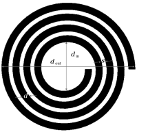
To prevent stress concentration in the inductor coil, the coil shape is designed to be circular, as shown in Figure 2.

FIG. 2 Schematic diagram of inductance structure
In the figure, dout is the outer diameter of the inductor coil, din is the inner diameter of the coil, s is the line spacing, and w is the line width. The commonly used theoretical calculation methods of inductance include the modified Wheeler formula, the current layer approximation method and the single data fitting expression [9], among which the modified Wheeler formula is simple and proved to be the closest to the measured value of inductance. The calculation formula of inductance based on this method is as follows:

Where: n is the number of turns of the coil; μ0 = 4π× 10-7; davg is the average diameter of the coil; dout is the outer diameter of the inductor; din is the inner diameter of the point inductor; Circular inductors are designed for K1 2.23 and K2 3.45.
The outer diameter of the design planar inductor is 9100μm, the line width is 200μm, the line spacing is 40μm, the line thickness is 7.5μm, and the number of turns is 12. The inductance value of the circular planar inductor calculated by Wheeler formula is 0.984μH.
1.3 Capacitor structure design
when the external pressure changes, the maximum deflection of the pressure-sensing film also changes accordingly.
In the figure, r is the radius of the sensitive film, t is the thickness of the sensitive film, d is the height of the capacitor cavity, p is the pressure load on the sensitive film, and ω is the deflection change of the sensitive film. For silicon materials, the maximum deflection of the center is

Where E and υ are Young's modulus and Poisson's ratio of materials.
The deflection of other points of the film can be expressed as

Where r is the distance from the point on the sensitive film to the center.
From the above formula, it can be seen that when the pressure sensitive film is deformed by external pressure, the deflection of the center of the pressure sensitive film is the largest, and the deflection of other points decreases with the increase of the distance from the center.
When subjected to external pressure, the maximum stress that the pressure sensitive film can withstand is

When designing capacitance structures, it should be noted that the maximum stress of the film is less than the yield stress of the silicon material. In order to protect the inductance structure, the capacitor inductance structure is designed in a sealed cavity, so the diameter of the sealed cavity should be slightly larger than the outer diameter of the inductance. Taking into account the test requirements, the resonant frequency of the designed sensor should be greater than 10 MHz. At the same time, with the increase of film thickness, the deformation of the pressure sensing film becomes smaller, the sensitivity decreases, and the increase of plate spacing will also reduce the sensitivity.

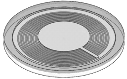
FIG. 4 Schematic diagram of sensor design structure
2 Preparation of the sensor
Because Si is a semiconductor, if the inductance preparation on Si will produce a large parasitic capacitance, thus affecting the sensor performance, so the inductance structure is prepared on BF33 glass. Because the resistivity of gold is small and the corrosion resistance is strong, the gold coil is conducive to surface cleaning, so the electroplating method is used to prepare the inductor coil. Si uses ICP to etch the travel pressure sensing film structure, and the specific production process is shown in Figure 5.
Steps 1-5 are carried out on the silicon wafer. The silicon wafer is chemically cleaned with acetone, alcohol ultrasonic and 3 # liquid successively, and silicon dioxide is deposited by PECVD on one side as an etching mask. BP212 photoetching capacitive cavity pattern, BOE etched SiO2 for graphic transfer, 42 μm by ICP to form a capacitive sealing cavity, the photoresist and silicon oxide were removed. The AZ4620 photoetching metal electrode pattern is carried out on the silicon, then 200 nm metal platinum is deposited, and the excess graphic metal is removed by lift⁃off process to form a metal capacitor top plate.
Steps 6-9 are performed on BF33, where BF33 is first chemically cleaned and the electroplated seed layer is deposited. AZ4620 photolithographic electroplating area, and then electroplating 7.5μm gold, inductor coil center is capacitor bottom plate, the photoresist is removed by acetone and RIE etching seed layer to complete the process on BF33.
Step 10 Anode bonding is performed between the silicon wafer and BF33, the silicon surface of the bonded wafer is thinned, and then the bonded wafer is sliced to complete the preparation of the sensor. After the sliced, the size of a single sensitive chip is 11 mm×11 mm× 0.66 mm.
3 Sensor performance test
In order to test the sensor, a resonant frequency-pressure test platform is equipped, as shown in Figure 6.
The resonant frequency-pressure test platform is mainly composed of Agilent E5061B network analyzer, Druck PACE600 pressure controller, vacuum pump and pressure chamber. The mechanical pump is connected to a pressure controller through which the pressure in the pressure chamber is controlled. The coupling chip and the sensor are fitted into the pressure cavity, and the two ends of the coupling inductance are connected to the test line by enameled wire. The data test is completed by reading the extreme value of the real part of the impedance corresponding to the resonant frequency on the network analyzer.
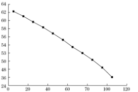
The relationship between the capacitance value and the distance between the upper and lower electrodes is nonlinear, the relationship between the pressure and the capacitance is also nonlinear, and the relationship between the resonant frequency and the pressure is also nonlinear. The resonant frequency of the sensor in the atmospheric environment is 46.95MHz, and the sensitivity is 161.5Hz/Pa, which has a high sensitivity.
4 Conclusion
In this paper, a high sensitivity wireless pressure sensor is designed, and its structure is designed by analyzing the detection principle to solve the problems caused by the traditional pressure sensor lead. The silicon wafer and BF33 glass are processed by a series of MEMS processes, and the size of a single sensitive chip prepared is 11 mm×11 mm×0.66mm. The resonant frequency-pressure test platform is built. The resonant frequency in atmospheric environment is 46.95MHz, and the sensitivity of the test sensor at normal temperature is 161.5Hz/Pa. The high sensitivity is conducive to improving the pressure detection accuracy.

FIG. 7 Resonance frequency-pressure test curve
References:
[1] Zhang Jianjun, Zhang Jianjun, Zhang Jianjun, et al ⁃ polymerization microsystem [J]. IEEE Transactions, 2006,31(6):1138-1159.
[2] Liu Jin, Owen, Gao Xuan. Research on MEMS passive wireless pressure sensor [J]. Instrument Technology and Sensor, 2013(11):4-6.
[3] Li Ying. Design, Manufacture and Test of LTCC High temperature Pressure Sensor [J]. Journal of Sensory Microbiology and Microsystems, 2013,32(4):101-102.
[4] Li Chen, Tan Qiang, Xue Chen, et al. A high-performance LC Wireless using passive pressure sensor Sintered Ceramic (LTCC) technology manufactured by Cryogenic co. [J]. Sensors, 2014,14(12): 23337-23347.
[5] Zheng Chao, Li Wei, Li Ailing, et al. Design and manufacture of passive pressure sensor based on LC resonance in China [J]. Mi⁃ Mechanical Engineering, 2016,7(5):87.
[6] Dong Ling, Wang Lifang, Huang Qingan. The realization of multipath adopts LC passive wireless sensor for parameter monitoring by stacking inductors with special winding [J]. Journal of Internet of Things, 2015,2(2):168-174.
[7] Li Haiyan, Cui Bin, Jin Shan, et al. Sensitivity ⁃ enhanced Letter of credit wireless bladder pressure sensor monitoring [J]. Journal of Sensors, 2016,16(12):1-1.
[8] Chen Peijun, Chen Zhiqiang, Chen Zhiqiang, et al. Implantation of flexible coil LC sensor based on wireless intraocular micromachining micro-invasive pressure sensing technology [J]. Journal of Microelectronics ⁃ Mechanical Systems, 2010,19(4):721-734.
[9] Li Jianjun, Li Jianjun, Li Jianjun, et al. Expression of simple and accurate planar spiral Inductance [J]. 1999,34 (10):1419-1424.
[10] Chen Peijun, Chen Zhiqiang, Chen Zhiqiang, et al. Implantation of flexible coil LC sensor based on wireless intraocular micromachining micro-invasive pressure sensing technology [J]. Journal of Microelectronics Fluid Mechanical Systems, 2010,19(4):721-734.


