Monocrystalline silicon high temperature piezoresistive pressure sensor
With the progress of semiconductor materials and technology, people have proposed a variety of structures of high temperature piezoresistive pressure sensors to solve the problem that conventional diffused silicon pressure sensors can not meet the requirements of high temperature pressure measurement, including: Polysilicon pressure sensor, SOS (silicon on sapphire) pressure sensor, SiC pressure sensor and SOI (monocrystalline silicon on insulator) pressure sensor, etc. The SOI mono-crystalline silicon pressure sensor realizes electrical isolation between strain resistors by SiO2, which solves the failure problem of PN junction isolation pressure sensor when the working temperature is higher than 125℃. At the same time, the superior piezoresistive effect of the top layer monocrystalline silicon film of SOI material and the good anisotropic corrosion characteristics of the bottom layer monocrystalline silicon film of SOI material can be used to fabricate the MEMS pressure-sensitive film structure. The high temperature piezoresistive pressure sensor technology is compatible with the conventional diffused silicon pressure sensor technology, easy to mass production, low cost, wide temperature adaptation. In addition, the sensor does not need peripheral cooling facilities, and has the advantages of small size, light weight and easy secondary assembly. Because there is no PN junction isolation problem, the sensor is not susceptible to optical, electromagnetic and ESD (electrostatic discharge) interference, and the noise related to PN junction is eliminated, which is conducive to improving the stability and reliability of the sensor.
1. Sensor chip design
The sensor core adopts a square diaphragm structure. The diaphragm deforms under the action of external pressure and transmits the pressure signal to the force-sensitive resistor on the diaphragm. The force-sensitive resistor changes the resistance value with the deformation of the stress diaphragm and converts the force signal into voltage signal output. The change of resistance is not only related to piezoresistive coefficient, but also related to stress size and distribution. The strain resistance arrangement of the pressure sensor is shown in Figure 1. After stress, the relative change of resistance is:

Where: π is piezoresistive coefficient; σ is stress.
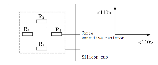
Figure 1 Strain resistance arrangement
The resistance values of the two groups are opposite to each other after the silicon diaphragm is acted on.
2 Sensor preparation
Based on the fabrication process of silicon based pressure sensor in Sensor National Engineering Research Center, the process flow of high temperature pressure sensor chip is designed. Compared with the OEM pressure sensor process, the differences are mainly reflected in the wafer material, electrode process and packaging process.
2.1 Oxygen injection isolation Technology (SIMOX) SOI wafer
SIMOX Technology SOI wafer process is shown in Figure 2. It mainly includes: (1) Oxygen ion implantation, which uses high-energy ion implantation equipment to generate a high concentration oxygen injection layer under the silicon surface layer; (2) High temperature annealing, the injected oxygen reacts with silicon, forming a buried SiO2 layer near the high concentration oxygen injection layer, and eliminating the damage introduced by ion implantation. The critical dose for oxide formation is about 1.4× 1018cm-2, and the typical injection dose is about 2× 1018cm-2. In order to avoid defects and stress introduction in high dose injection technology, the process was improved to multiple injection. The dose of oxygen injected is moderate and below the threshold dose for the formation of buried oxide layer. After a single injection and annealing, no continuous oxide layer was formed, and only oxide precipitates were formed near the range of oxygen ions. If the injection and annealing process is repeated 2 ~ 3 times, the total dose reaches the threshold dose. This can not only form a continuous oxide layer, but also reduce the defects and stresses induced in the silicon film during injection, so as to obtain high quality SOI material. The SIMOX technique makes the top silicon layer of the SOI material thinner, and the device layer of sufficient thickness can also be obtained through the epitaxial process.
2.2 Sensor chip technology
The cross-section of sensor chip fabrication process is shown in Figure 3. The process includes: silicon wafer cleaning → oxidation → photolitizing resistance strip → ion implantation → annealing → LPCVD deposition silicon nitride → photolitizing lead hole and silicon cup on the back → multilayer cladding
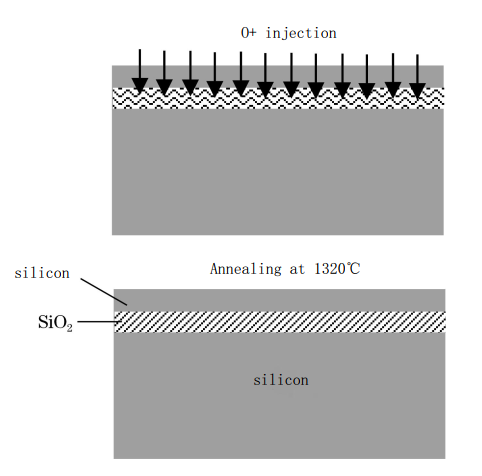
FIG. 2 SIMOX Technology SOI wafer process
Composite electrode preparation → Alloy → front graphic protection → back etching silicon cup → chip bonding with glass anode → split chip.
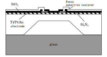
FIG. 3 Schematic diagram of sensor technology
Conventional pressure sensor uses Al electrode lead system, which is simple in process and low in cost. For the high temperature sensitive chip, the good ohmic contact between the bridge resistance is the guarantee of the reliability of the sensitive chip's electrical performance parameters. The working current of the pressure sensor is mA, the electrode is usually wide, and the Al electrode can ensure reliable operation when the working temperature is below 200 ℃. However, when the operating temperature exceeds 200℃, due to the action of thermoelectric stress, the degradation of Al/Si interface produces solution pits, and holes are easy to form at the contact, leading to debonding or virtual bonding. At the same time, the thermoelectric migration of Al to Si results in the stable operation of the ohmic contact deterioration sensor, which leads to the failure of the Al electrode lead system to guarantee the transmission. Therefore, a composite electrode system must be used as the electrode lead of the high-temperature pressure sensor. Ti-pt-au multilayer metallized electrode is used, Ti is used as the contact layer and adhesion layer, Pt is used as the barrier layer, and Au is used as the conduction layer. The working temperature can be as high as 400℃. The key of Cr-Ni-Au multilayer metallized electrode is the stress matching of each layer.
2.3 Pressure sensor assembly
When the chip is directly in contact with the measured medium or atmospheric environment, it will be sticky or absorb moisture, affecting the stability of the device. However, the backside compression encapsulation structure of the sensor has large nonlinear, and the fixed and closed edge structure of the signal conduction lead is complex, which will cause unforeseen problems. The sensor or sensor chip is isolated from the external environment by means of isolation diaphragm and isolation liquid, so as to protect the silicon chip from adverse factors in the external environment such as dust, moisture and other adverse effects. Drawing on the structure of OEM pressure sensor from the National Engineering Research Center of Sensors, the low stress rigid connection and protective fluid filling package technology are adopted. In order to reduce the additional pressure caused by the thermal expansion of the protective fluid, reduce the filling amount of the protective fluid, shorten the length of the inner lead wire, and improve the reliability of the internal structure, deep-hole sintered tube seat made of fusible alloy material is selected. The tube seat is concave structure, ceramic filler is embedded in the groove on the base, and the inner end face of the chip and the outer lead wire is in the same plane.
The packaging process of high temperature pressure sensor is shown in Figure 4. Whether the sensor can be used at high temperature and withstand long-term temperature cycle impact, packaging is the key to the success of sensor design and development. In order to ensure the accuracy of the pressure sensor and the long-term stability of the performance, eliminate the residual internal stress produced by the elastic sensitive element in the machining and heat treatment and the unstable factors such as the stress concentration formed by the assembly, the aging process such as temperature shock, device aging, pressure sensing film repeated loading and mechanical vibration is used to eliminate the residual internal stress and accelerate the release of internal stress. The pressure sensor performance tends to be stable.
3 Test results and analysis
In the performance detection under high temperature conditions, it is necessary to solve the high temperature resistance of the working medium of the pressure calibration device, and also to solve the sealing and thermal expansion coefficient matching technology between the fixture and the sensitive device, so that the test process does not introduce the system error due to the leakage and random interference of the test pressure. In view of the excellent penetration effect of gas, gas pressure gauge is usually used for pressure of micro pressure and medium pressure. When the high temperature fluorine rubber ring exceeds 250℃, the sealing effect will be reduced. The sensor and clamp are welded together by argon arc welding or electron beam welding technology to ensure the safety of testing under high temperature (high pressure, ultra-high pressure) conditions.
The static characteristics of the four sensors were tested repeatedly at 50, 100, 150, 200, 250 and 300℃, and the least square method was used for linear fitting of the test data. The results show that, in the temperature range of 50 ~ 300℃, the designed SOI monocrystal silicon pressure sensor has good static characteristics, the sensitivity is 29 ~ 33mV/MPa, the nonlinear error is less than 0.25% F·S, the repeatability is better than 0.2% F·S, which can be accurately measured in high temperature environment or for high temperature pressure. The relation curve between sensor sensitivity and temperature is shown in Figure 5. In the temperature range of 50 ~ 100℃, sensor sensitivity basically remains unchanged, indicating that within this temperature range, positive temperature coefficient of force sensitive resistor and negative temperature coefficient of piezoresistive coefficient complement each other well, and the designed doping concentration realizes self-compensation under constant current power supply. However, in the range of 100 ~ 300℃, the sensor sensitivity increases with the increase of temperature. The sensor sensitivity is affected by a variety of factors, such as compression resistance coefficient, force sensitive resistance temperature coefficient and additional stress of packaging structure. The sensor sensitivity increases with temperature, which can be corrected by using temperature compensation technology.
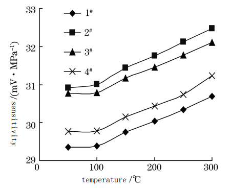
FIG. 5 Relation between sensor sensitivity and temperature
FIG. 6 shows the relationship between sensor nonlinearity and temperature. It can be seen that the nonlinearity of the four sensors decreases with the increase of temperature, which is consistent with literature [7], that is, the nonlinearity of piezoresistive effect decreases with the increase of temperature. Among the four sensors, the relation σ [110] between the resistance value of the force-sensitive resistor and the temperature is shown in Figure 7. At 50℃, the resistance value is about 4.6kΩ. In the range of 50 ~ 300℃, the resistance increases linearly with the temperature, showing good linearity. Therefore, the temperature resistance can be designed on the chip, and the temperature signal can be used to compensate the sensitivity of the pressure sensor, so as to further improve the performance of the high-temperature pressure sensor of SOI structure

FIG. 6 Relation between sensor nonlinearity and temperature
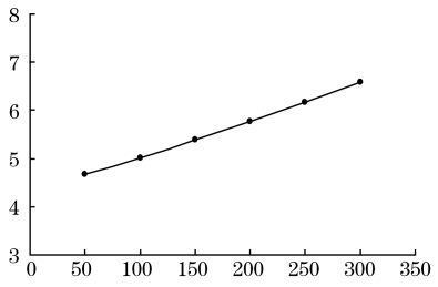
FIG. 7 Relation between resistance and temperature
4 Conclusion
Based on the silicon based pressure sensor production line of the National Engineering Research Center of Sensors, based on the oxygen injection isolation (SIMOX) technology SOI wafer, the development and testing of the monocrystal silicon high temperature pressure sensor was completed. The results show that the sensor has good static characteristics in the temperature range of 50 ~ 300 ℃, and can accurately measure the pressure or high temperature pressure in high temperature environment. With the improvement of material quality of SOI wafers and the development of manufacturing technology, high stability SOI monocrystal silicon high temperature pressure sensor will become the mainstream product of high temperature pressure sensor, and will also become the replacement product of conventional PN junction isolation pressure sensor.
It can be seen from the above measurement results that the scale coefficient of the sensor is 1.48μm/mV, with high sensitivity. However, the large return error near zero is caused by the DC biased output of the differential operational amplifier itself, which is about 9mV, about 3‰ of the full scale.
References:
[1] Chen Lifei, Yang Xiaorui, Guo Bingyang, et al. Optimal design of magnetic Liquid Micro-differential pressure sensor based on Pareto [J]. Journal of Yanshan University,2018,42(2): 151-158.
[2] Yu Zhisen, Yang Xiaorui, Zhang Ruixue, et al. Simulation Analysis and Experimental Study of Magnetic Liquid Inertial Sensor [j]. Instrument Instrumentation and Sensors, 2017(2):23-26. (in Chinese)
[3] Su Shuqiang, Li Decai. Research on Magnetic Liquid Inclination Sensor [j]. Acta Metrologica Sinica, 2016,37 (4) : 366-370.
[4] Rosenwig. Kinetics of hot metal [M]. Cambridge: Cambridge University Press, 1986.
[5] Liu Lotan, Xu Wei, Wang Shigang. Mathematical modeling of magnetic targeted drug delivery [j]. Journal of Shanghai Jiaotong University, 2008,42(1):1-4.
[6] Olaru, Petrescu, Hetanu. Research Progress of Magnetic Actuator [J]. Chinese Journal of Applied Electromagnetic Mechanics, 2010,32(1):267-274.
[7] Li Zhiqiang, Li Zejia, Li Zhiqiang, et al. Analysis of Ferrofluid Core Displacement Sensor [j] / / Electrical Machines and Engineering, 2010,34 (4): 357-357


